Nanostructure Materials & Devices Laboratory


Current Focus:

              On-Chip Quantum Nanophotonic Circuits comprising
                       • Single Photon Sources Array
                       • Photon Manipulation Circuitry


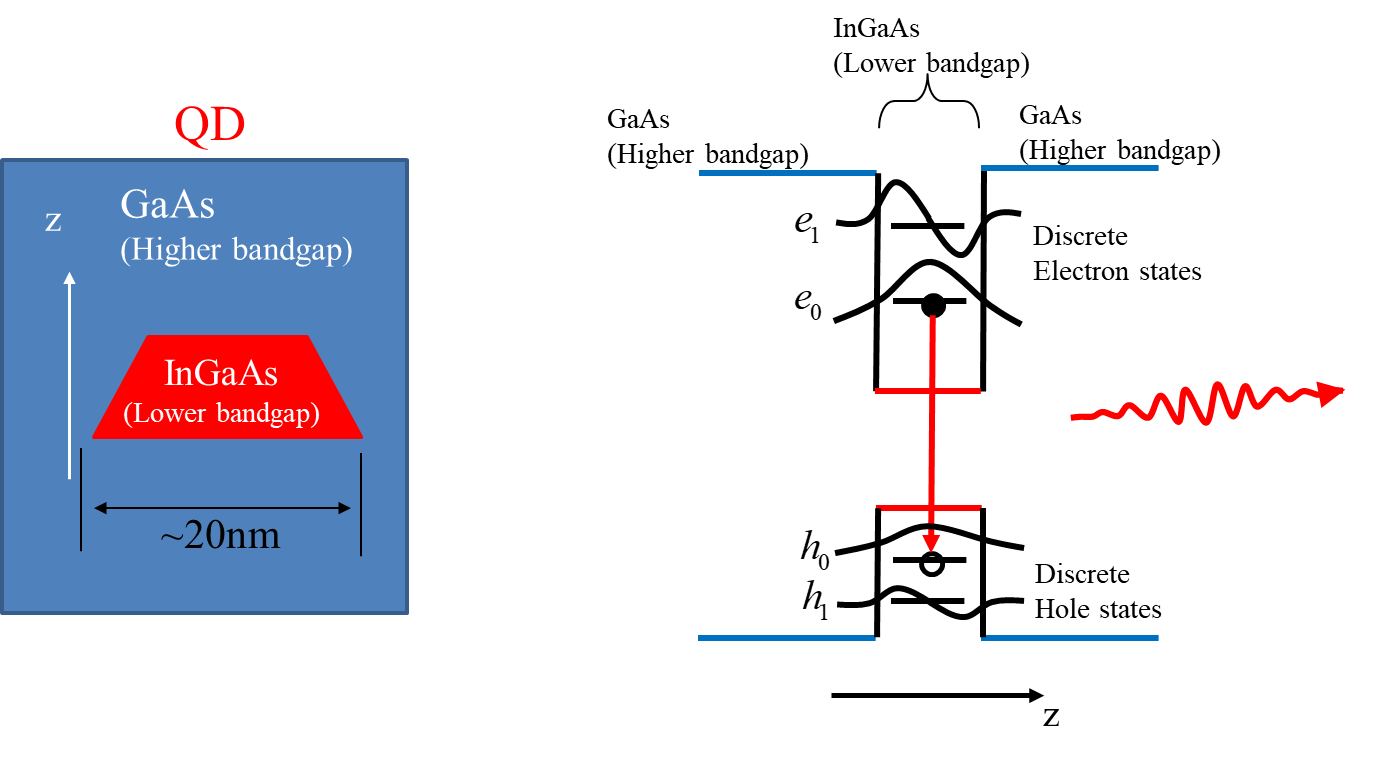
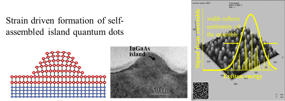
        We are focused on "Quantum Nanophotonics" that involves creating and studying on-chip quantum devices (shown below) and circuits that exploit the first quantum particle-- the photon-- for information sensing, transfer, and processing utilizing the rules of quantum mechanics. It is a foundational subset of the general field of "Quantum Information".


        We are using single photons as the quantum particle and create on-chip quantum nanophotonic systems (figure above) that exploit the rules of quantum mechanics for information sensing, imaging, communication, and processing beyond what laws of classical physics allow. Targeted areas of applications range from quantum imaging (i.e. spatial resolution determined by the Heisenberg uncertainty principle), metrology, quantum repeaters for long-distance secure communication, and quantum computing. Creating such systems that utilize as few as "single" photon to do the work requires following the laws of quantum mechanics for designing the systems and their 
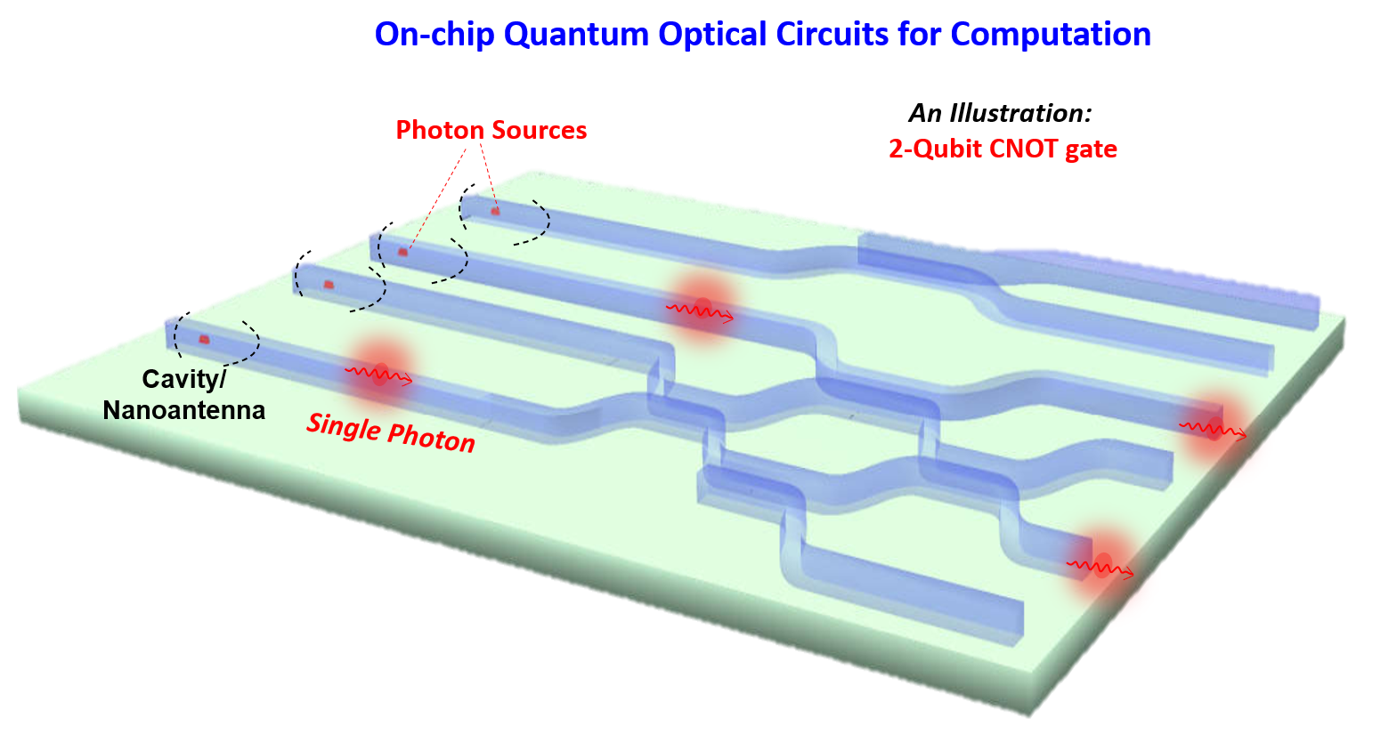
fabrication requires building blocks such as (1) photon sources generating single photons in a spatially ordered arrangement and (2) co-designed light manipulating units to control photons on-chip. All these components are to be fabricated at the nanoscale (typically from 10nm to 200nm) demanding parallel and well-coordinated efforts in the growth of appropriate combinations of materials with atomic-level control, their structural and chemical characterization, fabricating individual as well as interconnected devices (i.e. circuits) and studying their appropriate optical and electronic properties.

Our work on this involves two major fronts:
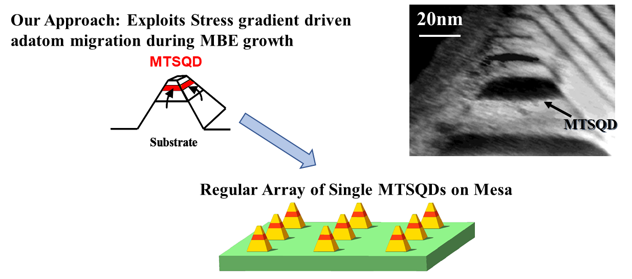
    (1) Developing the needed ordered on-chip integrable single photon source array utilizing a unique new class of mesa-top single photon sources
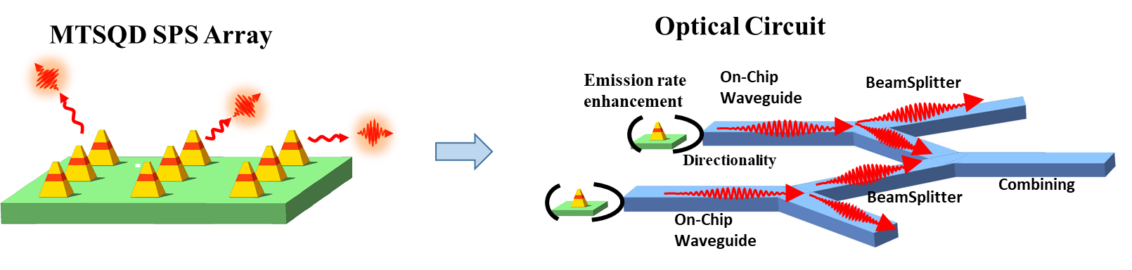
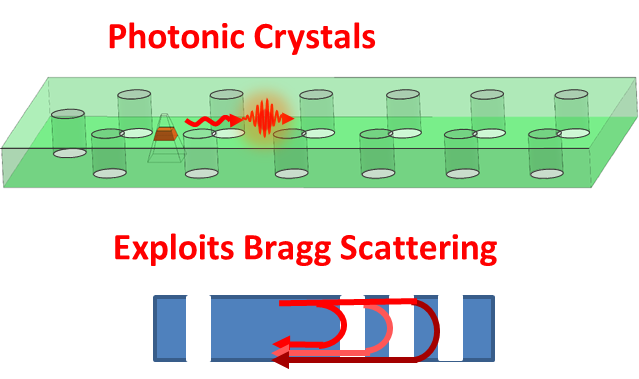
   (2) Developing the system level design of light manipulating units based circuitry to interconnect single photon source for circuits and device)


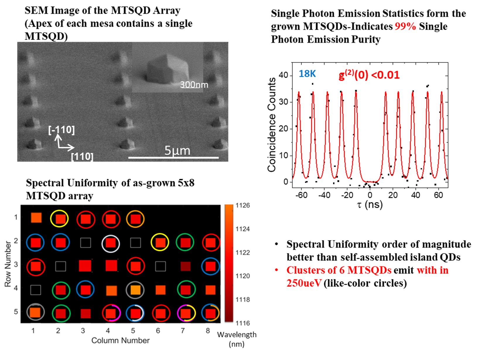
Single Photon Source Arrays:


  Why do we care about Single Photons?

    A single photon can act as qubit--a carrier for quantum information. The qubit may be encoded in the photon's polarization, number, phase, etc. Manipulation of single photons and their interference/ entanglement can result in Quantum Communication, Quantum Metrology, and Quantum Computation for Quantum Information Science.

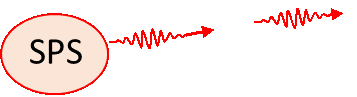
  What is so special about a Single Photon Source?

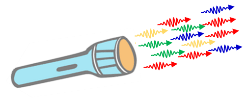
    Single photon sources emit only one photon at a time of only one color (/frequency).

Everyday photon sources:
-- Emit lots of photon of different (random) color.
Single Photon Sources (SPSs):
-- Emit only one photon at a time.
-- All the photons emitted are of the same color so that they can interfere/ entangle.

  Material Realization of Single Photon Sources-Quantum Dots:

    One of the ways to implement a single photon source is to create a 3D confined structure of a lower bandgap semiconductor surrounded by a higher bandgap one- Referred to as Quantum Dots. In a Quantum Dot, the electron and hole energy levels are discrete, thus enforcing it to emit only one photon at a time. For example the following picture schematically depicts a InGaAs QD surrounded by GaAs.

  Dominant approach to implement QD Single Photon Sources:

    Currently dominant approach to form QD Single Photon Sources is to form the quantum dots using lattice mismatch strain between two semiconductors during epitaxial growth such as MBE. This class of QDs are referred to as self-assembled island quantum dots.

Major Limitation:
-- --QDs are formed randomly on substrate, with locations.
-- High degree of size and shape fluctuation amongst the QDs, thus the emitted photons by different QDs are of random different frequency.
-- No way to couple the SPS to an optical circuit deterministically.

  Our approach: Single Quantum Dots formed on Mesas in regular arrays:

    We have pioneered a new approach to form the single QDs in regular arrays with uniform size and shape- exploiting engineered stress-controlled growth on Mesas- that allows integration to and scaling of the optical circuits. We name this new class of QDs as Mesa-top Single Quantum Dots (MTSQDs).

  Demonstrated Array of MTSQDs as Single Photon Sources:

    We have recently demonstrated this new class of QDs as spatially regular array of single photon sources!

    Check out our paper for more details:
    J. Zhang et.al, APL Photonics 5, 116106 (2020) [Link]
    J. Zhang et.al, Appl. Phys. Lett.114,071102(2019) [Link]
    J. Zhang et.al, J. Appl. Phys.120,243103(2016) [Link]


Photon Manipulation Circuitry:


  Manipulating the single photons emitted from the ordered array of SPSs for Quantum Information Processing:

    Let us now consider what is needed to build an on-chip MTSQD Single Photon Source based quantum information processing system. - We need an optical circuit to manipulate the emitted photons. Specifically-

  1. Enhancing the single photon emission rate.
  2. Enhancing single photon emission directionality to a specific direction
  3. On-chip propagation of the emitted photons
  4. On-chip splitting of a photon into different branches
  5. On-chip recombining of two photons from different SPSs- resulting in photon interference.

Such photon interference from different SPSs form the quantum information processing in the optical circuits.

   Two approaches: There are two dominant approaches in the literature to manipulate the emitted photons.

   (1) Bragg Scattering: Photonic crystals that exploit Bragg scattering of light by array of holes in a semiconductor membrane surrounding the QD to trap the photons in space-3D confined (Cavity), or 2D confined (waveguide).

<< This is a schematic of a single QD coupled to a photonic crystal waveguide.
Major Limitation:

--Need different components for the different light manipulating functions mentioned above.
-- Need to match between these components to form a larger optical circuit.

   (2) Mie Resonance: Exploiting collective Mie resonance of array of dielectric building blocks (DBBs):
Mie resonance are optical resonances in dielectric blocks when the size of the block is comparable to the wavelength/ refractive index. Coupling the Mie resonances of arrays of dielectric building blocks (DBBs) provide a unique way to achieve manipulation of light.
For example, following is a DBB array that functions as a nano-scale Yagi-Uda antenna (Nanoantenna)-enhancing the emission rate of the SPS, enhancing directionality and also propagating the photons.

  Multiple Functions using a collective Mie Resonance:

   In larger optical circuits based on DBBs, a single Mie mode can actually provide all the needed light manipulating functions for a working quantum optical circuit based on the single photon source. This provides a path to quantum information processing system based on photons as qubits- using on-chip interference and entanglement of the photons.

    Check out our paper for more details:
    S. Chattaraj et.al, IEEE Journal of Quantum Electronics 56,1, 1-9 (2019). [Link]
    S. Chattaraj, J. Opt. Soc. Am. B. 33, 12(2016) [Link]